Application-Oriented Testing of
SiC Power Semiconductors
Silicon carbide components offer many technical advantages and are suitable for demanding applications. However, there are structural differences between silicon components (Si) and SiC components. This affects reliability testing.
SiC (silicon carbide) has established itself as an important material in the semiconductor market because it has many outstanding properties. In comparison with silicon, SiC offers a higher electrical breakdown voltage, resulting in improved component performance and efficiency. It also allows for operation at higher temperatures, which makes heat dissipation easier and enables improved performance in a small space. Due to the high thermal conductivity of SiC, the components can be operated efficiently even under demanding conditions. The high switching frequency of SiC components allows for smaller and lighter designs, which is a major advantage in many applications. Thanks to these properties, SiC is used in an increasing number of industries, such as electromobility, renewable energies, industrial drive technology, and aerospace.
New Reliability Tests Required for SiC Power Semiconductors
However, these new SiC-based components will also require the development of new, specific reliability tests. The existing test methods and assumptions for silicon components cannot be used due to the structural differences between SiC and silicon. SiC has a different crystal structure, resulting in different electrical and thermal properties. If you ignore these differences, potential lifetime or performance limiting weaknesses may remain undetected. This article explains the relevance of new reliability tests for SiC-based power semiconductors using the dynamic gate stress (DGS) test procedure.
The DGS test is primarily used for SiC-FET (field-effect transistors). In this test procedure, a stress signal in the form of a square wave signal is applied to the test object at the gate with the maximum and minimum gate voltage of the DUT (device under test). During the stress cycles, active temperature control is used to adjust the DUT to the desired stress temperature. The stress is paused at defined intervals in order to measure the gate threshold voltage and the RDSon of the DUT.
In the case of test procedures for wide-bandgap semiconductors, there are significant differences between dynamic and static stress methods. A test system from SET GmbH is used for the test procedure described in this article. The exact test specifications are explained on the basis of this test setup and the resulting measurement results are compared with practical applications. The correct measurement process also plays an important role in achieving reliable and reproducible measurement results. In this context, reference is made to the ECPE (European Center for Power Electronics) Guideline AQG 324, which provides a code of practice and guideline for new test procedures for SiC components in Europe.
Dynamic Gate Stress (DGS) Test: Functional Principle and Measurement Process

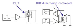
In the DGS process, an FET is connected to the ground potential at its drain and source contacts, and stressed at its gate contact (Fig. 1). The stress signal itself is defined in the Guideline AQG 324. The parameters of the stress signal are as follows: The amplitude of the square wave signal is the maximum negative and positive voltage that may be present according to the specifications for the desired DUT. The rise time (dV/dt) at the DUT should be in the order of 1V/ns and the stress frequency should be greater or egal 50khz with a duty cycle in the range of 20% to 80%.
The duration of stress depends on the frequency, therefore a higher frequency may reduce the test time. According to the Guideline AQG 324, the stress duration should be greater than or equal to 10^11 cycles. The test is carried out at an actively and tightly controlled temperature of 25°C.
As part of this test procedure, the gate threshold voltage, and the RDSon resistance are measured during fully automated stress breaks. Precise measurement and the appropriate preconditioning process are of great importance during this process. Preconditioning is used to ensure that the condition of the test object is identical for each measurement and therefore that the measurement results are comparable. In this context, the Guideline AQG refers to the JEDEC Guideline JEP184, which describes the correct process for the measurements. The defined voltage at the gate should correspond to either the recommended gate-source useful voltage or the maximum/minimum permissible gate-source voltage.
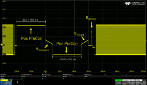
A common used preconditioning time is 100 ms, but it is sometimes also significantly longer. After this period of time, the measurement of the gate threshold voltage should be carried out quickly—as a guide value, the measurement should take place within 10 ms. The oscilloscope recording shown was recorded with a DGS system from SET GmbH and it is used here to explain the measurement process.

The curve in Figure 2 corresponds to the gate signal. At the start you can see the stress phase at -10 V to +22 V at 300 kHz, which then pauses because the measurement process begins. The measurement process starts with a positive 22 V precondition pulse, which is maintained for 100 ms. The gate voltage is then constantly changed in very small steps. During this test phase, the I-drain current is measured and set to a certain value, for example, 20 mA. The 20 mA can flow at the start of the “Vth(down)” test phase because the FET is turned on. As soon as the gate voltage comes close to the threshold voltage, the FET slowly closes and the current that was previously able to flow completely through the FET slowly decreases. When I-drain has reached a defined current value, for example 10 mA, the gate voltage is saved as Vth(down). The same measurement procedure is repeated for the negative area: In this case there is a minimum gate voltage of -10 V for 100 ms. The gate voltage is then gradually increased and the Vth(up) voltage is saved at 10 mA.
After completing the Vth measurements, the Rds(on) resistance of the test object is measured. An adjustable current pulse is generated between drain and source for this purpose. The Rds(on) resistance is determined by measuring the voltage drop between drain and source. After these measurements are completed, the dynamic gate stress test is continued. A reliable implementation of this procedure is crucial for accurately characterizing the behavior of the SiC semiconductors under stress and for ensuring their reliability.
Assessment of DGS Measurement Results Compared with Static Measurements
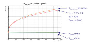
Extensive comparative tests were carried out in order to evaluate the need for a DGS test and to compare this with a conventional static test procedure. Conventional 1200 V SiC MOSFETs with a RDSon of 80 mΩ were used as test objects during this process. These MOSFETs are all of the latest generation and are currently available on the open market. The maximum recommended gate voltages at a stress frequency of 100 kHz and a duty cycle of 50% from the data sheets were used as stress parameters for the following tests. The entire test process was carried out under laboratory conditions at a stable 25°C.

The analysis of the data obtained indicates an enormous difference between the static and dynamic test procedures (Fig. 3). The graphical representation shows notable differences, particularly in relation to the drift of the gate threshold voltage. In the dynamic tests, a significant drift of over 4 V in the gate threshold voltage was identified after 300 giga-cycles. This drift effect was not observed in the static tests. Considering that standard MOSFETs have a drift of around 0.5 V, this drift is 700% higher than usual. For many circuits, this increase may result in significant deterioration in performance or even circuit failure. SET GmbH has repeatedly been able to identify these deviations in dynamic tests; no evidence of drift of this kind was found in static tests.

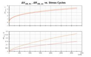
Further investigation was carried out into the correlation between a change in the gate threshold voltage and the RDSon resistance. Figure 4 illustrates a clear relationship between the threshold voltage drift and the RDSon resistance based on the measurement results of the first test in the previous figure. As can be assumed, when the gate threshold voltage shifts, the RDSon resistance also changes according to the characteristic datasheet curve of the component. During operation, this has an impact on the efficiency of the component and therefore, for example, also on the range of an electric car. The specific effects in the operating conditions can be estimated based on the continuous measurements during the test.
In order to constantly improve understanding of the phenomena of SiC power semiconductors, both DGS tests and all other dynamic test procedures must be developed further and continued. For the modeling of long-term analyses in particular, it is essential to collect as much data as possible in order to be able to develop reliable power semiconductors for the challenges of the future.
Author: Gabriel Lieser, SET GmbH


